This clearance is usually determined by the oxide transition time across the well boundary. May be viewed as the size of minimum feature.
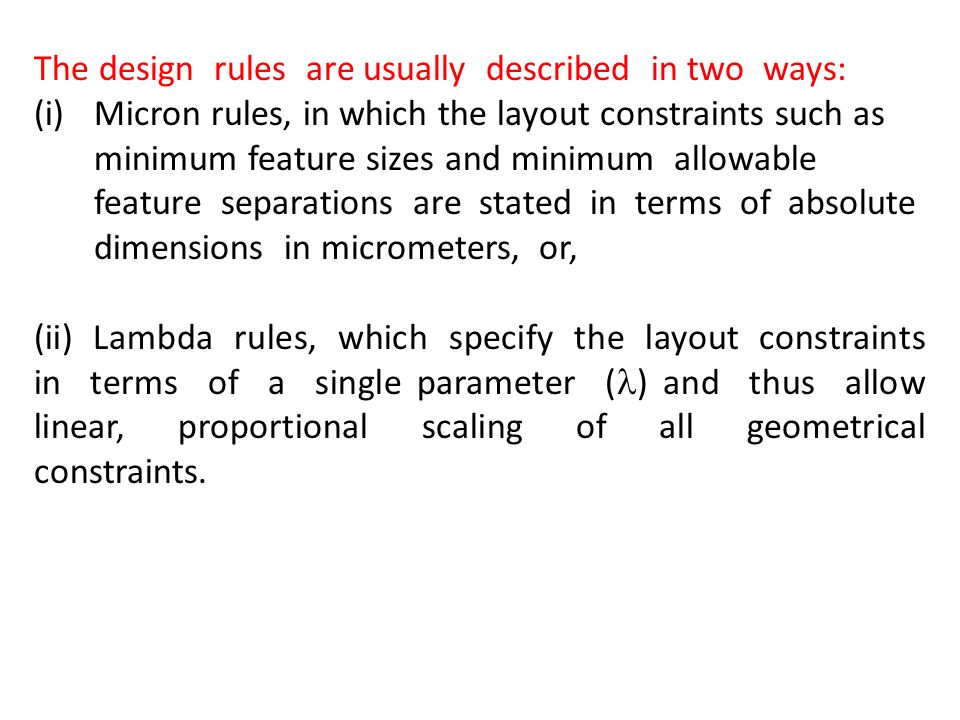
Design Rules
For micron rule sets it is set by the foundry and for 013µm technology is 0005µm.

. The value of lambda is half the minimum polysilicon gate length or λ L2 and L being the minimum dimension of polysilicon gate fabricated in each technology node. Wire widths to avoid breaks min. The appropriate figure may be calculated as.
𝐹 2 𝜀 0 2𝜀 𝐹 2 1012 𝐹 𝐹 108 2 The typical area capacitance values for 5μm MOS circuits are. Simplified micron rules with limited scaling attributes. O Mead and Conway provided these rules.
Let us consider scaling pharosc 2µm layout to generic 013µm rules. Design Rules CMOS VLSI Design Slide 5 Feature Size Feature size improves 30 every 2 years or so 12 07 reduction factor every generation from 1 μm 1000 nm in 1990 to 14 nm in 2015. 10 generations in 20 years 1000 700 500 350 250 180 130 90 65 45 32 22 14 10 nm 0 10 20 30 40 50 60 70 80 90 2005 2010 2015 2020 2025 2030.
If the lambda snap grid is 1 with. Provide feature size independent way of setting out mask. VLSI DESIGN 1080502 29 Design Rules2 Two major approaches.
The rules provide details for the minimum dimensions line layouts and other geometric measures which are obtained from the limits of certain dispensation expertise. Clearance between n-well edges and n diffusion should be good enough. Lambda λ parameter used in magic.
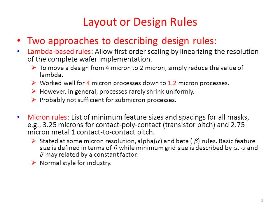
Lambda Based Design Rules. Allow first order scaling by linearizing the resolution of the complete wafer implementation. Micron rules.
The term VLSIVery Large Scale Integration is the process by which ICs Integrated Circuits are made. Design rules represents a tolerance which insures very high probability of correct fabrication scalable design rules. Micron Based Design Rule.
The other rule is grounding n-well providing sufficient number of well taps. UNIT- II VLSI DESIGN Page 8 Normally area capacitances are given in pF μm2 where μm micron 10-6 meter 10-4 cm. 4 e List out the back-end steps in ASIC design flow.
Stated at micron resolution. Two different lambda rule sets used by MOSIS. N-well is deeper mounted than any other transistor implants.
DESIGN RULES UNIT II CIRCUIT DESIGN PROCESSES Two major approaches. Two approaches to describing design rules. Design rules based on single parameter λ.
3 d Explain the concept of driving large capacitive loads with relevant examples. These design rules are quantified in μm or in lambda λ units. B Compare and contrast the Lambda based and Micron based Rules for layout design.
In the SCMOS rules circuit geometries are specified in the Mead and Conways lambda based methodology 1The unit of measurement lambda can easily be scaled to different fabrication processes as semiconductor technology advances. What is micron design rule. O Lambda is a unit and can be of any value.
1 Design Rules Rules for constructing fabrication masks 2 Chip design file a GDSII binary format universally used today b CIF text readable format used primarily by academic tools in the past Units commonly used in design rules 1 absolute dimensions micron rules 2 scalable design rules. To move a design from 4 micron to 2 micron simply reduce the value of lambda. Design rules represents a tolerance which insures very high probability of correct fabrication not a hard boundary.
The rules are specifically some geometric specifications simplifying the design of the layout mask. 7292018 ECE KU 12 What is Lambda Based Design Rule o Setting out mask dimensions along a size-independent way. Therefore lambda-based design rules are simply not useful for sub-micron CMOS technologies.
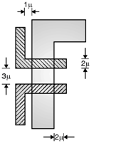
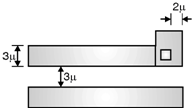
Width of pMOS should be twice the width of nMOS. Click to enlarge image Click to enlarge image Figure-32. Stated at micron resolution.
These rules help the. Layout Design rules Lambda Same N and P alters symmetry L min Wpmos2 Wnmos. Lambda Based Design Rule Micron Based Design Rule.
Allow first order scaling by linearizing the resolution of the complete wafer implementation. Simple for the designer. 11 SCMOS Design Rules.
The lambda snap grid multiplied by the lambda scaling factor must be a multiple of the micron snap grid. A simple comparison with the lambda- based rules shows that there are significant differences. 4 c Draw and explain the schematic of Pseudo-nMOS Inverter.
Where a 025 m gate length is quoted is 0125 microns m. Micron rules can result in as much as a 50 size reduction over lambda rules. The pharosc rules used for the rgalib vgalib vsclib and wsclib.
VLSI designing has some basic rules. Normal style for industry. O Mask layout is designed according to Lambda Based.
Simplified micron rules with limited scaling attributes. DESIGN RULES Design rules define ranges for features Examples. The Alliance sxlib rule set scaled from 1µm to 2µm.
Layout or Design Rules. 3 f Write about Programmable IO blocks in FPGAs. Minimum distance rules between device layers eg polysilicon metal metal metal diffusion diffusion and minimum layer overlaps are used during layout Layout design rule checker DRC automatically verifies that no design rules have been broken.
List of minimum feature sizes and spacings for all masks eg 325 microns for contact-poly-contact transistor pitch and 275 micron metal 1 contact-to-contact pitch. For lambda rule sets the value chosen directly impacts the available lambda scaling factor. Worked well for 4 micron processes down to 12 micron processes.
A generic 013µm rule set. Spacing to avoid shorts minimum overlaps to ensure complete overlaps Measured in microns Required for resolutiontolerances of masks Fabrication processes defined by minimum channel width Also minimum width of poly traces Defines. There are two basic rules for designing.
O According this rule line widths separations and extensions are expressed in terms of. The MOSIS design rule numbering system has been used to list 5 different sets of CMOS layout design rules.

Vlsi Circuit Design Process
Micron Design Rules Digital Cmos Design Electronics Tutorial
Micron Design Rules Digital Cmos Design Electronics Tutorial
Purpose Of Design Rules Ppt Video Online Download
Vlsi Circuit Design Process
Layout Design Rules 2 Introduction Layout Rules Is Also Referred As Design Rules It Is Considered As A Prescription For Preparing Photomasks Ppt Download

Lambda Based Design Rule Hindi Youtube

What Are Different Types Of Design Rules
0 comments
Post a Comment